Intel 18A Makes Its Official Debut, with Two Heavyweight Chips Unveiled
Intel 18A, two cutting-edge technologies
Before introducing these two chips, let’s first take a look at Intel’s highly anticipated Intel 18A process, which integrates two game-changing technologies. According to Intel, the Intel 18A process is
the first 2nm-class node developed and manufactured in the United States. Compared with the Intel 3 process, it delivers a 15% improvement in performance per watt and a 30% increase in chip
density. This node was developed, qualified for manufacturing, and entered early production at the company’s factory in Oregon, with mass production set to begin later this year.
So, what makes this generation of process so special? Let’s start with a principle in the chip industry named after Intel co-founder Gordon Moore — Moore’s Law.
In the author’s understanding, the core of Moore’s Law essentially states that the number of transistors per unit area of a chip will double within a certain time cycle. However, to achieve these goals,
the chip industry has exhausted various methods. For instance, in terms of transistors, the industry has driven their evolution from planar architecture to FinFET over the past few decades. But when
moving to process nodes below 3nm, adopting Gate-All-Around (GAA) technology has become the goal for all wafer manufacturers.
RibbonFET, which is first used in Intel 18A, is a representative of such GAA transistors. Intel stated that RibbonFET is the company’s first new transistor architecture in more than a decade, enabling
greater scalability and more efficient switching, thereby enhancing both performance and energy efficiency.
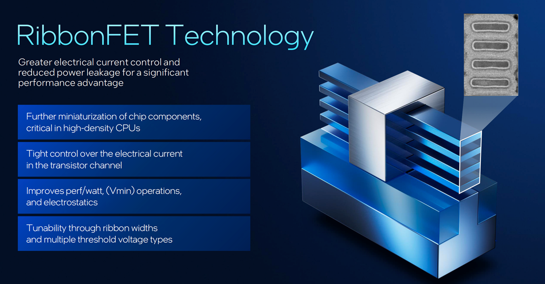
Intel experts previously highlighted in a press release that "RibbonFET may be the most complex transistor ever manufactured."
As one expert explained, "RibbonFET continues the geometric revolution by flipping the fin of the FinFET and stacking it vertically, allowing them to be densely arranged like 'ribbons' (with pitch scaling down from around 30 nanometers to 10 nanometers). The effort is worthwhile: the gate wraps around the ribbon structure, enabling the transistor to perform better. Overall, each transistor switches faster (higher performance), operates more efficiently (lower power consumption), and occupies less space on the wafer. This represents the fulfillment of Moore's Law."
In addition to the new transistor, another highlight of Intel 18A is the groundbreaking backside power delivery system, PowerVia, which enhances power flow and signal transmission.
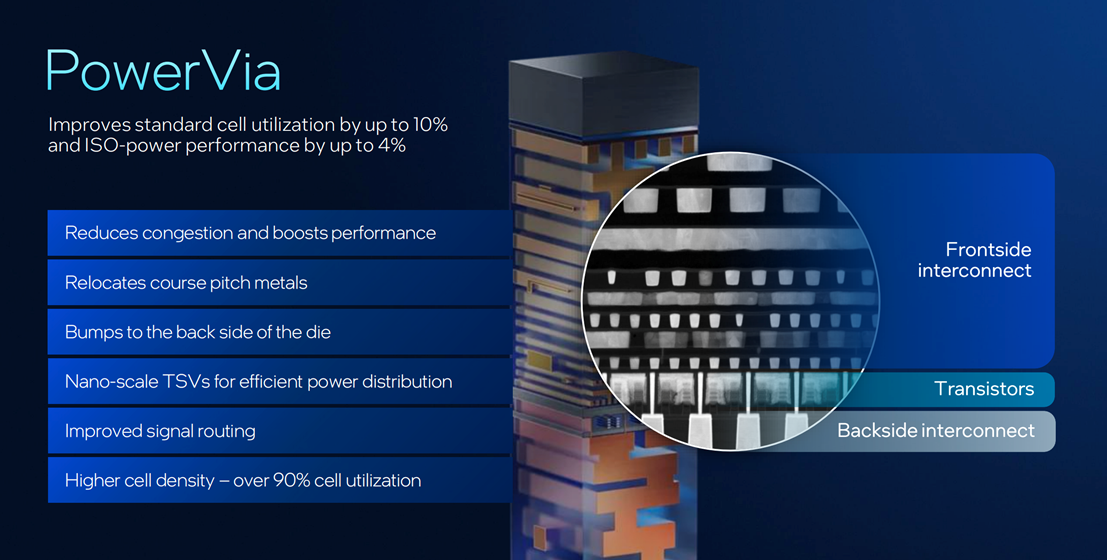
In traditional semiconductor designs, both power (VDD/GND) and signal interconnects are routed through multiple layers of wiring at the top of the silicon wafer. However, as
transistor sizes shrink and wiring density increases, this front-side configuration leads to heightened routing congestion, voltage drop, IR drop, and reduced power efficiency,
making it difficult to meet signal integrity and performance targets. In response to these challenges, the industry has shifted toward backside power delivery, and PowerVia is
Intel's proprietary Backside Power Delivery Network (BSPDN) technology.
In Intel’s view, the benefits of this technology and approach are multifaceted, far outweighing the increased complexity introduced by the new process.
"For example, power lines can occupy up to 20% of the frontside area. Therefore, removing these power lines eases the burden on the interconnect layers—this relief is significant enough to offset the costs associated with the entire advanced process. By simplifying the most cumbersome part of the manufacturing flow, the end result is that the two-step flipped process is actually more cost-effective than previous ones," Intel emphasized.
Furthermore, as Intel has demonstrated, when combined with advanced packaging and the 3D chip stacking technology Foveros, Intel can stack and integrate multiple chips into advanced System-on-Chip (SoC) designs. This delivers flexibility, scalability, and performance at the system level.
In the newly launched Clearwater Forest and Panther Lake, Intel has fully leveraged its manufacturing advantages to their greatest extent.
Panther Lake, a comprehensive upgrade
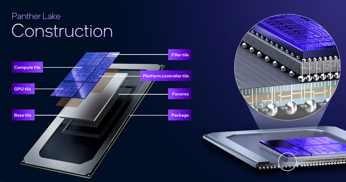
As Intel’s first Intel 18A-based AI PC processor, Panther Lake is undoubtedly a chip that combines both performance and energy efficiency. In terms of configuration, as shown in the diagram, Intel’s "Panther Lake" is mainly composed of five tiles, namely the Compute Tile, GPU Tile, Base Tile, Filler Tile, and Platform Control Tile. These tiles are then integrated together using Intel’s leading Foveros 2.5D packaging technology to create a highly competitive System-on-Chip (SoC).
Gao Song, Vice President of Intel's Client Computing Group and General Manager of Intel China, summarized the key features of this chip during its introduction, stating that the
processor series as a whole boasts four major strengths:
Panther Lake combines the high energy efficiency of Lunar Lake and the high performance of Arrow Lake. By integrating the advantages of both, Panther Lake has become a product series that excels in energy efficiency, delivers outstanding performance, and offers strong scalability. Specifically, Panther Lake achieves a graphics card performance improvement of up to 50%; its NPU (Neural Processing Unit) performance has also been significantly enhanced, thereby boosting overall AI capabilities substantially.
"This represents progress not only in TOPS (Trillions of Operations Per Second) figures—rising from over 40 TOPS in Lunar Lake to 50 TOPS in Panther Lake—but also in the reduced area of the NPU chip," Gao Song explained. "While the smaller area may not be directly reflected in performance tests, it is of great significance for lowering manufacturing costs."
Panther Lake has also made considerable strides in wireless connectivity, with greater flexibility in Wi-Fi, Bluetooth, and even 1GbE MAC technology. "We have adopted Wi-Fi 7 R2, the industry's most advanced wireless technology, to integrate AI PCs with stronger connectivity performance. This will significantly optimize the user experience," Gao Song added.
As previously mentioned, Intel's leading manufacturing process is the key to this chip's outstanding performance. Beyond that, Intel's iterative innovations in architecture and cores are also indispensable factors driving the improvements in this new processor.
First, regarding the Compute Tile, reports indicate that this tile contains P-cores (Cougar Cove) and E-cores (Darkmont), NPU 5, IPU (Image Processing Unit) 7.5, memory interfaces, and a Xe media and display engine separated from the graphics block. Among these, the x86 architecture-based Cougar Cove and Darkmont are undoubtedly the most critical components of Intel's processor, representing the very foundation upon which Intel's processor business is built.
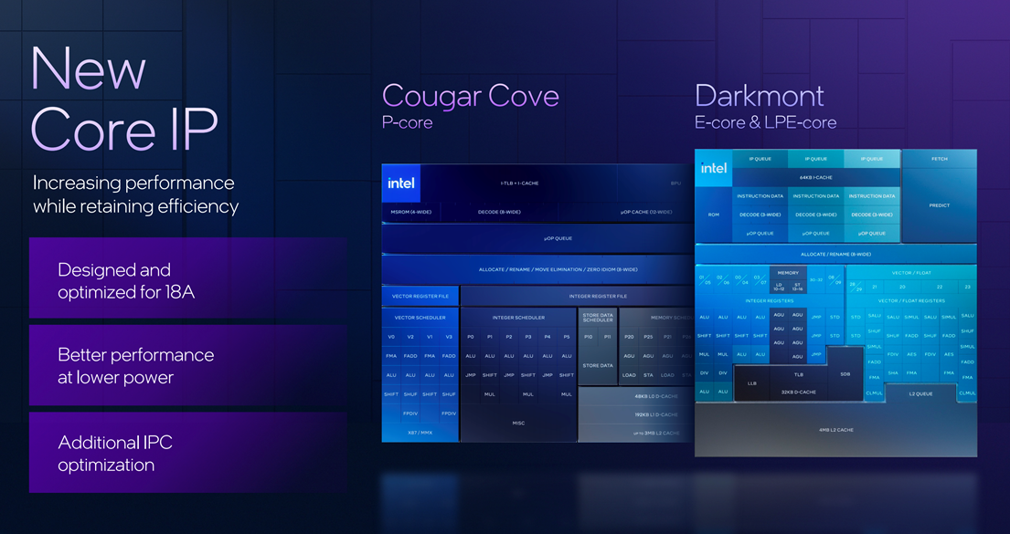
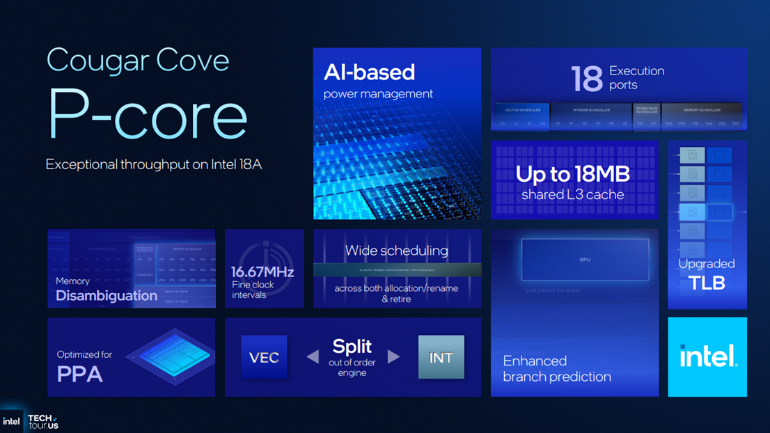
For the Performance core (P-core, codenamed Cougar Cove), Intel has indicated that the improvements to this new core are primarily typical enhancements to the existing CPU architecture—such as an upgraded branch predictor and a translation lookaside buffer (TLB) with increased capacity. As Intel stated, “We did not change the width or the depth; instead, we focused on optimization.” The company also emphasized, “Cougar Cove now adopts an AI-based power management approach, which dynamically adjusts the aggressiveness of certain functional units (e.g., prefetchers) based on the requirements of different workloads.”
Intel further noted that the shift to the 18A process has enabled it to advance some infrastructure within Cougar Cove, and the TLB is among the key beneficiaries. According to Intel, a larger TLB allows more complex workloads to run faster and more reliably.
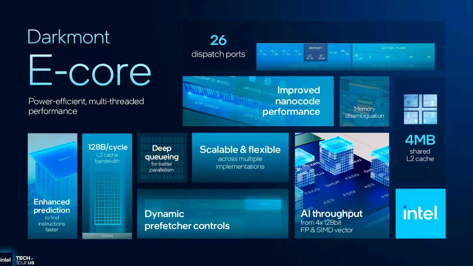
Moving on to the Efficiency core (E-core, codenamed Darkmont), Gao Yu, General Manager of Intel China's Technology Department, explained that as an iterative version of Skymont, Darkmont's updates focus on three key stages: the front-end, the out-of-order execution core, and the back-end execution ports. Intel has achieved significant improvements in all three stages. As shown in the diagram, Intel has comprehensively enhanced the front-end components such as the decoding unit and instruction queue of this core, as well as the out-of-order execution core and back-end execution ports. It is precisely the comprehensive optimization of these three stages that has enabled the Darkmont efficiency core to achieve a significant increase of over 10% in IPC (Instructions Per Cycle).
Additionally, as can be seen from the previous introduction, Panther Lake also features an LPE core (Low-Power Efficiency core). According to Gao Yu, in this new-generation processor, this core is placed on a separate power island with independent power management. Moreover, its cache configuration and operating frequency are optimized based on its low-power positioning. It is precisely this design that allows its operating frequency and power consumption performance in real-world applications to be adjusted according to the overall platform design, thereby achieving an optimal balance between performance and energy efficiency.
Next, looking at the GPU Tile, it specifically refers to the new-generation GPU—Xe3— which is capable of multi-frame generation (i.e., inserting AI-generated frames between actually rendered frames).
Intel stated that the Xe3 GPU has been redesigned to enhance scalability. Within the GPU’s rendering slices, Intel has increased the number of Xe cores from 4 to 6, upgraded the L1 cache (Level 1 Cache) from 192 KB to 256 KB, and expanded the L2 cache (Level 2 Cache) from 8 MB to 16 MB. These improvements reduce the need to access local memory while boosting performance. Intel also noted that the Xe3 GPU adopts a variable allocation strategy for its allocated threads, which has a significant impact on performance.
Turning to multi-frame generation, as shown in the diagram, Intel previously introduced XeSS 2 (Xe Super Sampling 2), which is designed to accelerate graphics processing for video games. Specifically, XeSS’s frame generation feature inserts an AI-generated frame between two "real" rendered frames and uses low-latency technology to offset the latency caused by this process.
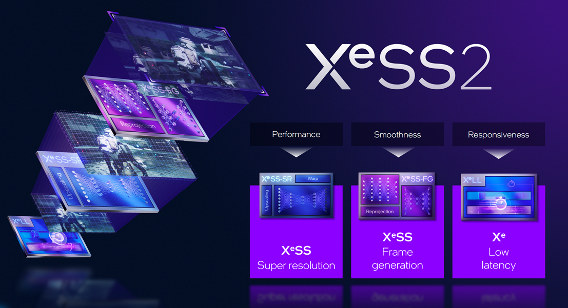
With the launch of Panther Lake, Intel has introduced the XeSS-MFG (XeSS Multiframe Generation) feature. This feature can be combined with existing upscaling and multiframe generation technologies to inject up to three additional interpolated frames. According to Intel, in practical applications, users can control this feature as part of Intel’s existing graphics software package—they may choose to set additional frames manually or allow the application to decide automatically.
Notably, the software will also offer options such as specifying how much system memory to share with the GPU. This is of great significance for AI applications and even certain games.
When it comes to the introduction of this technology, one aspect that cannot be overlooked is the latency introduced by frame generation. In this regard, Intel explains that gamers' experience of latency can be summarized as the delay between user input and perceived motion. To address this issue, solutions such as using AI to predict mouse movements or adjusting the variable rate of rasterization to AI-rendered frames can be implemented.
Intel has also launched a pre-compiled shader distribution, allowing your computer to download pre-compiled shaders directly from the cloud instead of waiting for shader compilation. Furthermore, Intel is developing Intelligent Bias Control 3.0, which enables the CPU and GPU to communicate with each other and allocate power to the appropriate logic. As a technology that complements Thread Director, it can boost GPU performance by at least 10%.

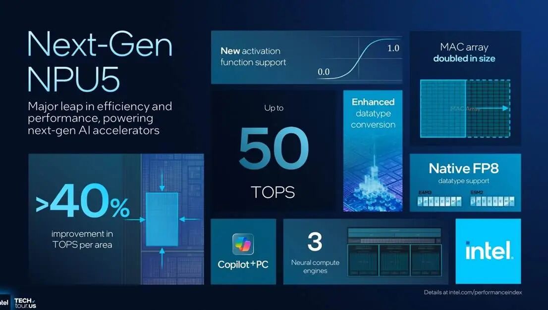
Turning to the NPU (Neural Processing Unit) aspect, Gao Song explained that Intel’s NPU 4 has achieved a major breakthrough in energy-efficient performance. In terms of chip area, the new-generation accelerator has been reduced by 40% year-on-year, bringing advantages in cost and integration. In terms of computing power, the new-generation accelerator reaches 50 TOPS (Trillions of Operations Per Second), representing a significant improvement over the previous generation. Additionally, this NPU natively supports FP8 (8-bit floating-point) precision, which provides better support for large language models (LLMs).
From a data perspective, the NPU 5 integrated into Panther Lake features 4.5MB of scratchpad RAM, 256KB of L2 cache, and 6 SHAVE DSPs (Digital Signal Processors). Intel pointed out that the most significant change in Panther Lake’s NPU 5 lies in further improvements and adjustments to its MAC (Multiply-Accumulate) array. According to reports, the number of MACs per unit area has doubled, which has increased the TOPS per unit area by 40% compared to the Lunar Lake NPU.
Thanks to these leading cpus, igpus and Npus, Intel can provide extensive support for AI tasks on PCS. Gao Yu also reaffirmed: "Intel adheres to the XPU route, meaning that cpus, igpus, and Npus all need to be utilized, working in coordination and each performing its own duties." " The CPU is good at responding quickly, so for those models that have high requirements for response speed, we recommend running them on the CPU, such as voice-to-text conversion. And what are the characteristics of a GPU? Its bandwidth is relatively large, so those who have high demands for bandwidth should run on a GPU. The characteristic of NPU is its high energy efficiency ratio, so those who pursue energy efficiency should run on NPU. Gao Yu went on to say.
According to reports, the CPU delivers 10 TOPS of computing power, the iGPU provides 120 TOPS, and the NPU contributes 50 TOPS, enabling Panther Lake to handle a wide range of AI tasks with exceptional ease and efficiency. Beyond these computing chips, as mentioned earlier, various connectivity, display, and media components also form essential parts of Panther Lake's architecture.
Thanks to these advanced configurations, Intel has developed the following three Panther Lake-based products:
An 8-core chip featuring 4 P-cores and 4 low-power (LP) E-cores;
4 Xe3 GPU cores and 4 ray-tracing units;
Memory interfaces supporting 6800 MT/s LPDDR5X or 6400 MT/s DDR5.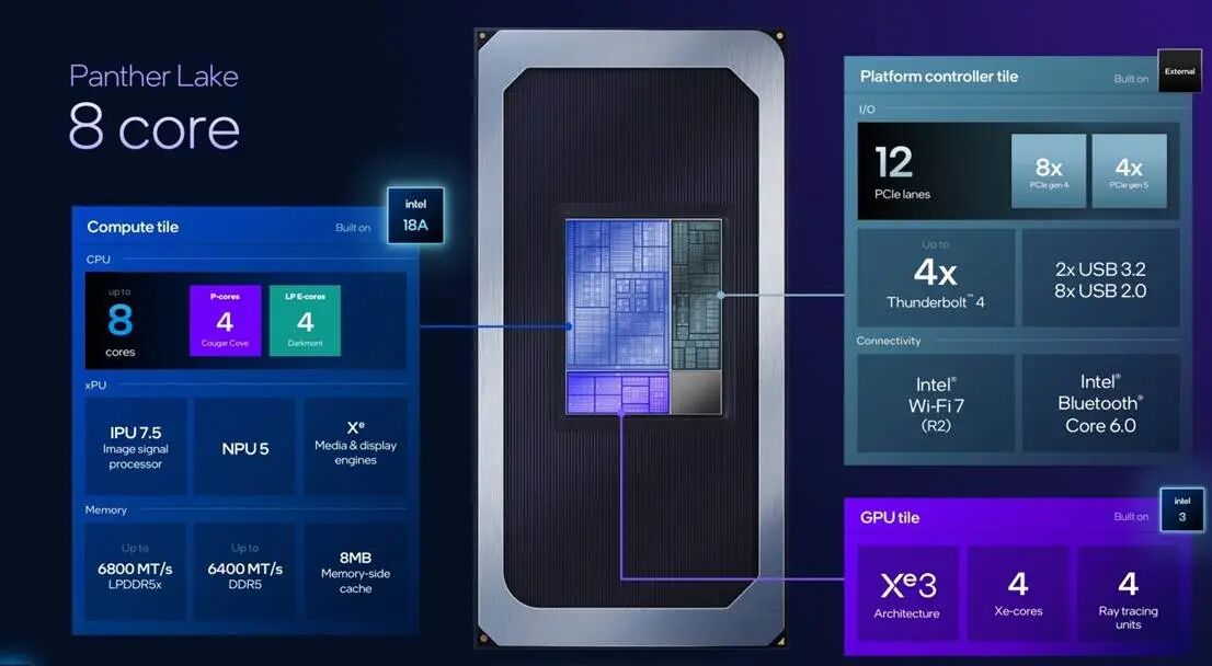
A 16-core chip featuring 4 P-cores (Performance cores), 8 E-cores (Efficiency cores), and 4 LP E-cores (Low-Power Efficiency cores); it is equipped with 4 Xe3 GPU cores and 4 ray tracing units. For memory interfaces, it supports either 8533 MT/s LPDDR5x or 7200 MT/s DDR5.
A 16-core chip configured with 4 P-cores, 8 E-cores, and 4 low-power (LP) E-cores, along with 12 Xe3 GPU cores and 12 ray-tracing units. It features a memory interface supporting 9600 MT/s LPDDR5X.
Notably, as shown in the diagram, the 8-core Panther Lake chip will feature 12 PCIe lanes (8 PCIe 4 lanes and 4 PCIe 5 lanes), while the 16-core chip will come with 20 PCIe lanes (8 PCIe 4 lanes and 12 PCIe 5 lanes). By contrast, the 16-core 12Xe Panther Lake chip will have its PCIe lane configuration reduced to 12, matching that of the 8-core model.
Intel emphasized that Panther Lake introduces a scalable multi-chip architecture, providing partners with unprecedented flexibility across various specifications, market segments, and price points. This architecture supports a wide range of devices, including consumer and commercial AI PCs, gaming equipment, and edge solutions. Among these, edge applications—including robotics—are also a key focus for Panther Lake. Intel revealed that its new Intel Robot AI Software Suite and reference boards will enable customers with advanced AI capabilities to leverage Panther Lake for rapid innovation, developing cost-effective robots for control and AI/perception tasks.
“Mass production of Panther Lake will begin this year. The first SKUs (Stock Keeping Units) are expected to ship before the end of this year, with broad availability starting in January 2026,” Intel stressed.
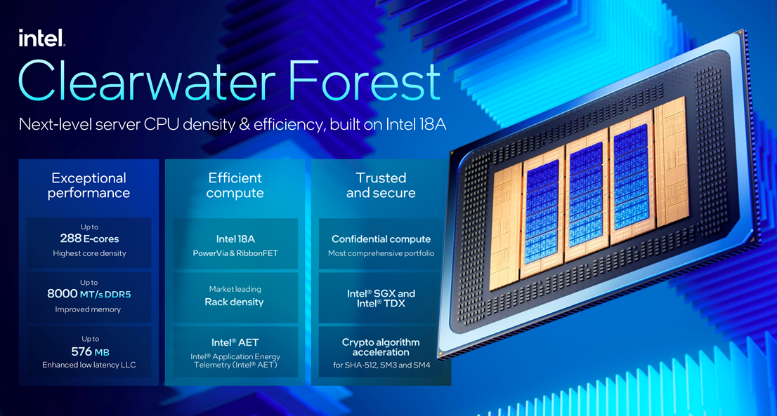
Clearwater Forest is a 288-core E-core processor.
At this year’s Intel Tech Tour (ITT), Intel also unveiled the successor to its data center-focused Sierra Forest—the Xeon 6+ CPU product, designed based on E-cores (Efficiency cores). Looking back at Intel’s past layout for its Xeon lineup, this may mark the beginning of Intel subdividing its Xeon product line into two series: the P-core (Performance core) series and the E-core series.
According to reports, Clearwater Forest, built on the all-new "Darkmont" efficiency core, adopts a multi-layered solution comprising multiple chiplets and building blocks—making it a major engineering achievement for Intel. By combining significant architectural upgrades with the latest 18A process technology, advanced 3D Foveros packaging, and EMIB (Embedded Multi-die Interconnect Bridge) technology, Intel has created its most efficient server processor to date. And it is precisely with the launch of Clearwater Forest that Intel has elevated its disaggregated architecture and packaging design to a new level.
Let's take another look at the Darkmont E-core.
According to the introduction, this core mainly relies on a wider, more parallel front-end and an enhanced out-of-order execution engine. Meanwhile, each core of Darkmont is equipped with a 64 KB instruction cache and features expanded decoders, enabling it to process more instructions per cycle than the previous-generation Crestmont E-core. As for its reordering and allocation structures, improvements have also been made. Additionally, the number of allocation units has been increased, and the out-of-order window has been expanded to accommodate more in-progress work. Furthermore, the execution resources have been doubled, and the execution ports for integer and vector operations have been significantly increased—this allows the core to maintain higher parallel throughput.
From a design perspective, Intel states that a Clearwater Forest is composed of 12 EMIB tiles in a 2.5D package. These tiles connect three active base tiles together, which are then linked to two I/O tiles and a total of 12 compute tiles. Among them, the I/O modules are built using the Intel 7 process, the active base tiles are fabricated with the Intel 3 process, and the compute chipsets are manufactured on the Intel 18A process node.
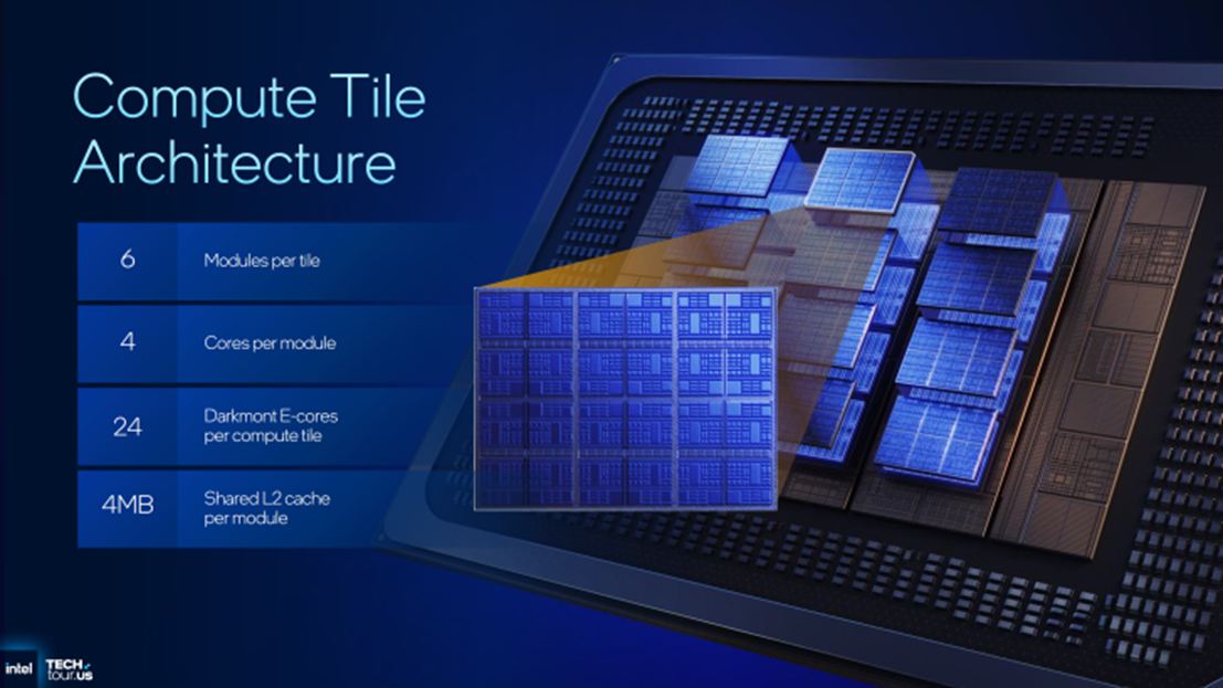
First, let’s look at the compute tiles. As shown in the diagram, each compute tile consists of 6 modules, and each module contains 4 Darkmont E-Cores. In this way, each compute tile has 24 Darkmont E-Cores, and the 12 compute tiles together have a total of 288 E-Cores. Each module also includes 4 MB of L2 cache, which means each compute tile has 24 MB of L2 cache, and the 12 compute tiles have a total of 288 MB of L2 cache. This brings the total L3 + L2 cache of the entire chip to as high as 864 MB.
Next, let’s look at the I/O Tiles. According to the introduction, each I/O Tile of Clearwater Forest provides 48 PCIe Gen 5.0 lanes (totaling 96 lanes), 32 CXL 2.0 lanes (totaling 64 lanes), and 96 UPI 2.0 lanes (totaling 192 lanes).
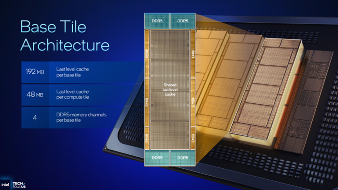
As for the three Active Base Tiles, they are manufactured using the Intel 3 process. Each Base Tile is equipped with four DDR5 memory controllers, resulting in a total of 12 memory channels on the chip. Notably, this module also includes a shared LLC (Last-Level Cache): each Compute Tile has 48 MB of LLC, and each Base Tile has 192 MB of LLC, which enables the provision of an on-package LLC capacity of up to 576 MB. These Tiles are connected to the Compute Tiles above them using EMIB (Embedded Multi-die Interconnect Bridge).
From Intel's introduction, we learn that Clearwater Forest is also its first mass-produced CPU to adopt Foveros Direct 3D technology. As an advanced packaging solution, Foveros Direct 3D enables the connection of compute tiles and I/O tiles on active base tiles. With a bump pitch of 9 micrometers and the use of copper-to-copper bonding technology, Foveros Direct 3D serves as a high-density, low-resistance active silicon interposer, delivering a performance of approximately 0.05 pJ/bit. In other words, this means Intel can transfer data between two chips with almost no power consumption. By combining EMIB (Embedded Multi-die Interconnect Bridge) with Foveros chips, Intel is able to connect heterogeneous components in Clearwater Forest, thereby creating a package design that incorporates a large number of active chips.
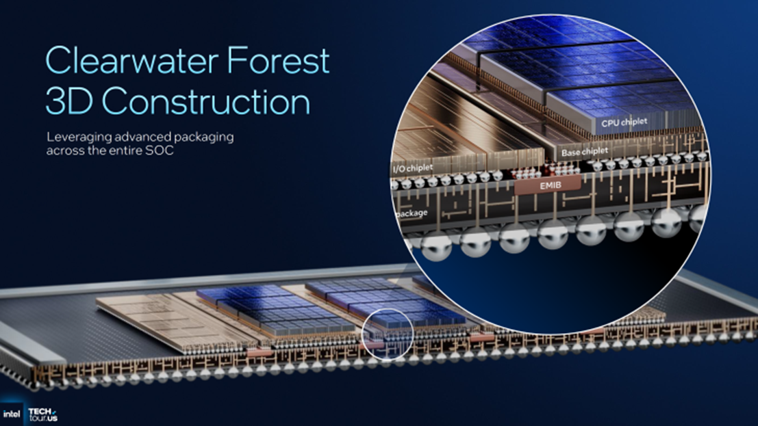
In summary, the specifications of Clearwater Forest are outlined below. Intel highlights that compared to the previous generation, Clearwater Forest achieves a 17% improvement in Instructions Per Cycle (IPC), along with significant enhancements in density, throughput, and power efficiency. Tailored for hyperscale data centers, cloud providers, and telecommunications companies, Clearwater Forest enables organizations to scale workloads, reduce energy costs, and deliver smarter services.
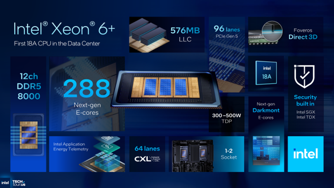
From a platform perspective, Intel's Clearwater Forest CPU will support 1S (1-socket) and 2S (2-socket) configurations with the LGA 7529 socket. It also includes Intel Software Guard Extensions (SGX) and Intel Trust Domain Extensions (TDX). In terms of power management, Clearwater Forest will be equipped with Intel Application Energy Telemetry (AET) and Intel Turbo Rate Limiter. Finally, the Clearwater Forest CPU will feature Advanced Vector Extensions 2 (AVX-2) and support Vector Neural Network Instructions (VNNI) as well as INT8 (8-bit integer).
It is reported that Clearwater Forest is compatible with the current Xeon 69xxE/P platform, allowing the reuse of existing servers while retaining 12 memory channels and extensive PCIe and CXL support. As memory speeds advance toward DDR5-8000, Intel has also announced system specifications—such as a maximum of 288 cores per socket, a dual-socket upper limit of nearly 576 cores, and a combined last-level cache (LLC) of over 1,152 MB across the entire package.
Written at the end
Based on the above announcements, it is evident that Intel has not only made significant strides in chip design and manufacturing but has also demonstrated its commitment to listening to customer needs and implementing necessary strategic adjustments to maintain competitiveness. While both the PC and server markets are maturing, new competitors continue to emerge, requiring Intel to remain strategically focused to retain its leadership position.
As Intel CEO Dr. Pat Gelsinger stated in the company press release: "We are entering an exciting new era of computing, driven by leaps in semiconductor technology that will shape the coming decades. Our next-generation computing platforms, combined with our leading process technologies, manufacturing, and advanced packaging capabilities, will serve as catalysts for innovation across our businesses as we build the new Intel. The United States has always been home to Intel's most advanced R&D, product design, and manufacturing — and we are proud to build upon this legacy, expand our U.S. operations, and bring new innovations to market."
Although the transformation will not happen overnight, with these products and technologies, Intel has already embarked on a new journey to reclaim its leadership.


